

Abstract
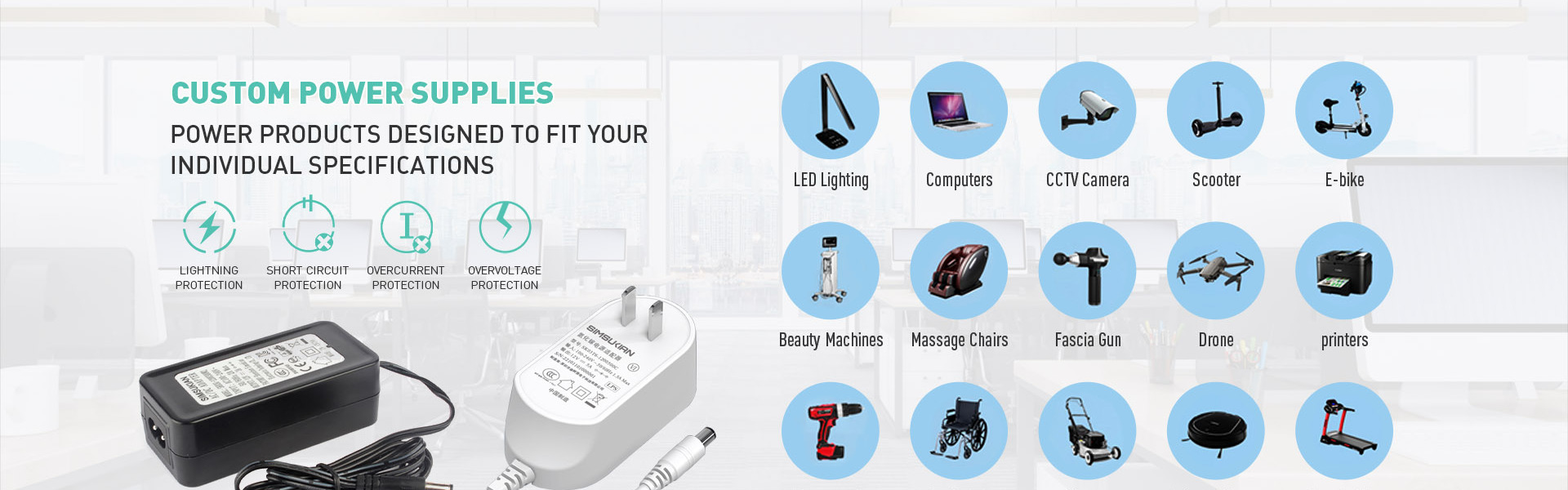
GaN devices in a GaN fast charger switch far faster than silicon. Common-mode current and radiated emission of the GaN fast charger become harder to control. From transformer shielding and PCB layout to input filtering, each part of the GaN fast charger must be redesigned for high dv/dt.
1. High dv/dt and Common-mode Current
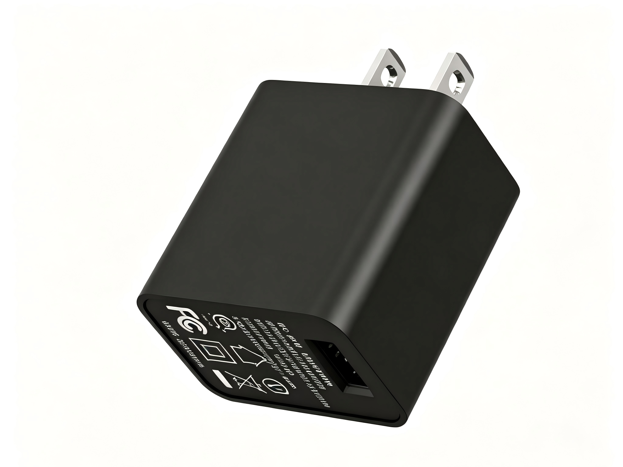
Switching times of GaN devices in the GaN fast charger are in the nanosecond range, with drain-source slew rates reaching tens of volts per nanosecond, far above silicon MOSFETs. Fast transitions in the GaN fast charger couple through transformer parasitic capacitance, thermal pads and PCB capacitance into the housing and cables, forming common-mode current. The noise spectrum of the GaN fast charger extends higher in frequency, beyond what low-band filtering covers.
2. Conducted Emissions and Input Filtering
Conducted emissions of the GaN fast charger are measured over the specified band with quasi-peak and average limits, Class B being stricter. Differential noise in the GaN fast charger comes from input current pulsation, common-mode noise from the parasitic paths above, and the two need X capacitors and common-mode chokes respectively. If self-resonance of filter parts falls below the noise band, attenuation of the GaN fast charger drops sharply, so high-frequency behaviour matters more than low-frequency insertion loss.
3. Radiated Emissions and PCB Antenna Effects
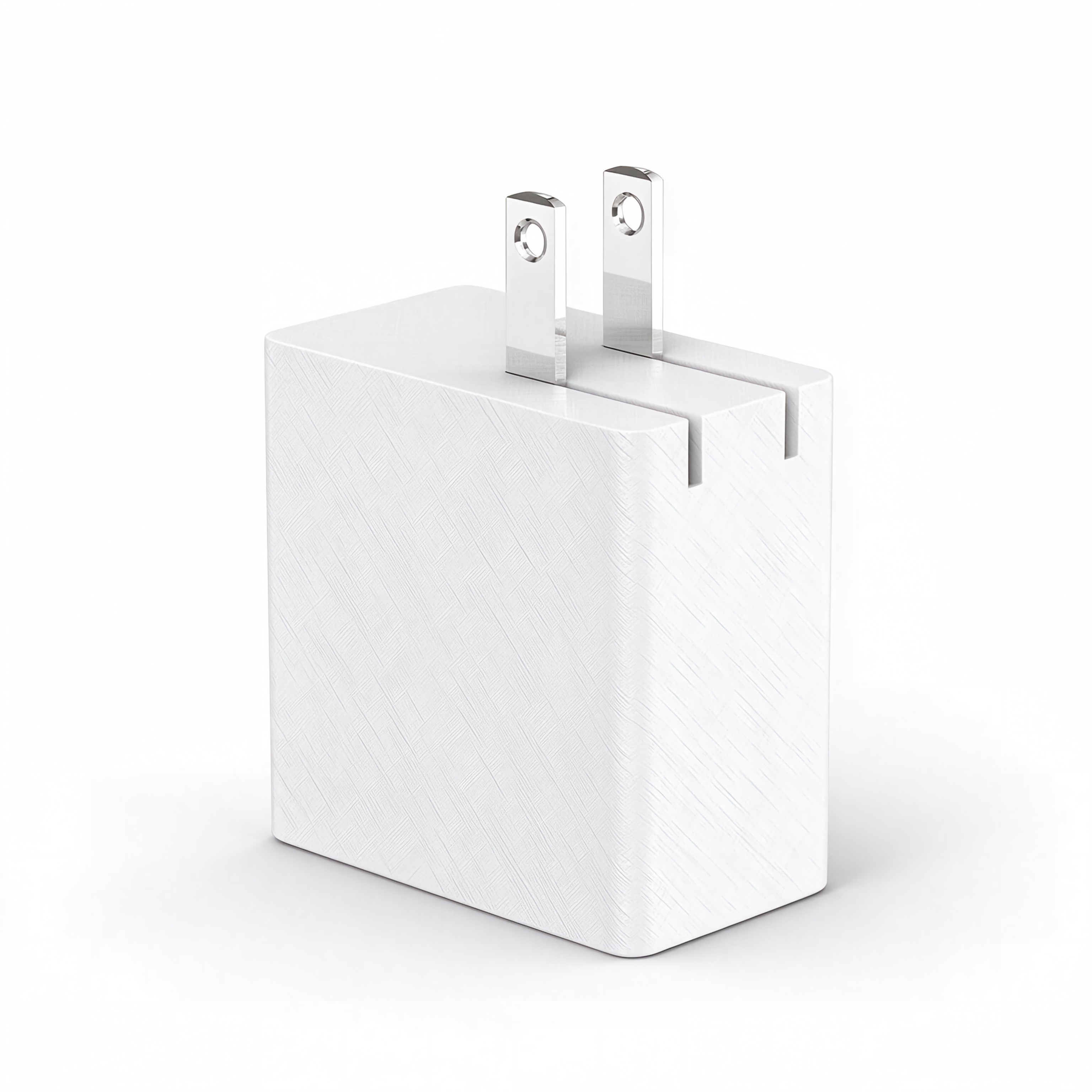
Small size brings power loops and housing closer in the GaN fast charger, so traces and internal cables easily act as antennas. Switching node copper area, transformer leakage flux and output cable length all shift radiation peaks of the GaN fast charger. Layout shortens high di/dt loops, encloses switching nodes within power ground and avoids long parallel runs, adding shielding between devices and housing when needed.
4. Snubber Circuits and Shield Windings
To suppress spikes and ringing, the GaN fast charger often adds RC or RCD snubbers across the switch, with values affecting both noise spectrum and efficiency. Larger snubber capacitance lowers dv/dt in the GaN fast charger but raises switching loss, requiring a trade-off with thermal design. A shield winding tied to a quiet primary node reduces common-mode current of the GaN fast charger, and its connection must coordinate with Y capacitor positions to avoid new resonance.
5. Test Setup, Margin and Corrective Order
EMC results of the GaN fast charger are setup sensitive: height, grounding, cable routing and chamber background all shift readings. The GaN fast charger should keep sufficient margin so batch variation in cores or devices does not cause failure. Corrective work starts at the noise source before filter and shield tuning, since enlarging Y capacitors in the GaN fast charger raises leakage and needs a safety re-check.
Conclusion
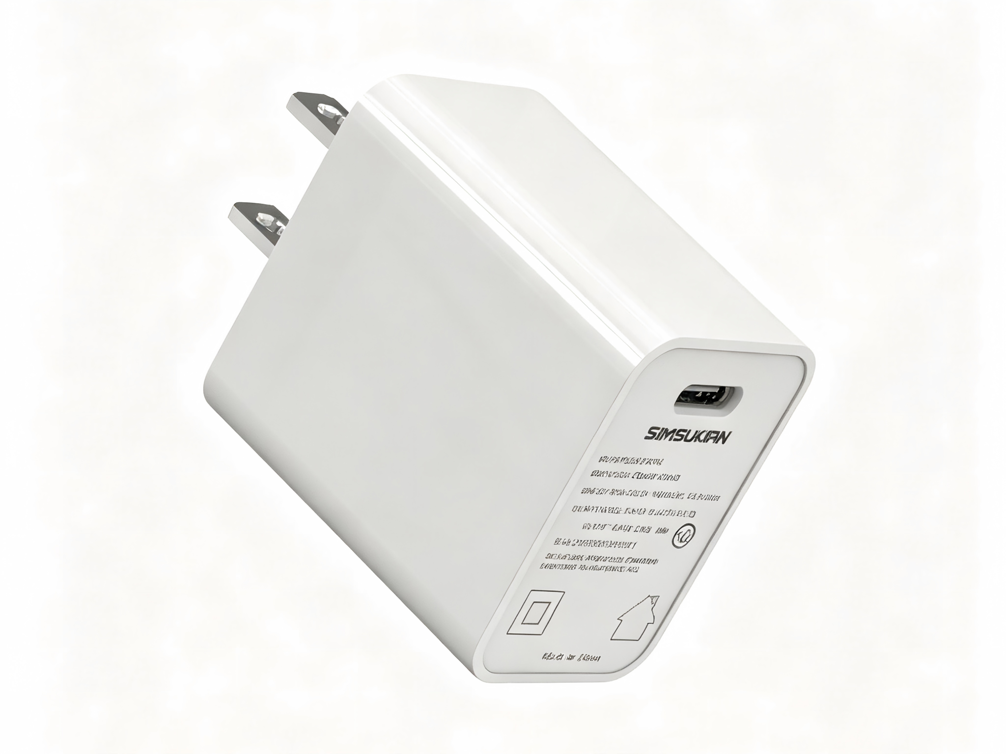
EMC difficulty of a GaN fast charger stems from high-speed switching itself; adding filters late rarely gives stable compliance. Simsukian provides EMC pre-testing against EN 55032. Overseas buyers are welcome to contact Simsukian to confirm test and corrective paths for the GaN fast charger.
FAQ
Q1: Are the certifications complete and verifiable?
A1: Simsukian’s full product range covers major certifications including UL, CE, FCC, PSE, KC, SAA, UKCA, and CB. All certificates can be verified through official channels, effectively avoiding risks of fake, borrowed, or expired certificates that may cause customs clearance failure or platform delisting.
Q2: How is the quality stability and protection performance?
A2: All Simsukian products undergo 100% aging tests and are equipped with multiple protections including over-voltage, over-current, short-circuit, and over-temperature protection. They feature low ripple, low heat generation, and an average lifespan of approximately 50,000 hours, supporting long-term full-load stable operation.
Q3: Can products be customized? What are the sample and mass production lead times?
A3: OEM/ODM customization is fully supported, including voltage, current, connector, plug type, housing, and logo. Sample lead time is 5 days. Standard bulk order lead time is 18–20 days. Sample fees are refundable after placing a bulk order.
Q4: Do the products meet energy efficiency and standby power requirements?
A4: The full range meets DOE Level VI and higher energy efficiency standards. Some models achieve no-load power consumption ≤0.1W, complying with ErP and other international energy-saving regulations.
Q5: How are lead time, MOQ, and after-sales service guaranteed?
A5: As a source manufacturer with abundant stock of standard models, delivery is stable. Standard warranty is 1 year (free repair within the first year). Lifetime repair support is provided; after the first year, appropriate material and labor fees will be charged.
References
1. Simsukian Official Website
2. EN 55032 Electromagnetic compatibility of multimedia equipment – Emission requirements
3. IEC 61000-4-4 Electrical fast transient/burst immunity test
Power adapter
Power adapter
Related Articles More>>
- Plastic Enclosure Flame Rating and Aging Test Parameters of USB charger
- Under-Voltage Input Protection for Charger: Equipment Safety for Low-Grid-Voltage Conditions
- Energy Compliance of Wall-Mount Power Adapter: No-load Power and Average Efficiency Calculation
- Convertible Plug Power Adapter vs Fixed-Plug Adapter - Selection Comparison Technical Parameters