

Abstract
GaN devices in a GaN fast charger have low threshold voltage, so the GaN fast charger is prone to gate false turn-on under high dv/dt. Drive voltage window, gate resistance and common-source inductance layout are key reliability factors of the GaN fast charger.
1. Low Threshold and False Turn-on Risk
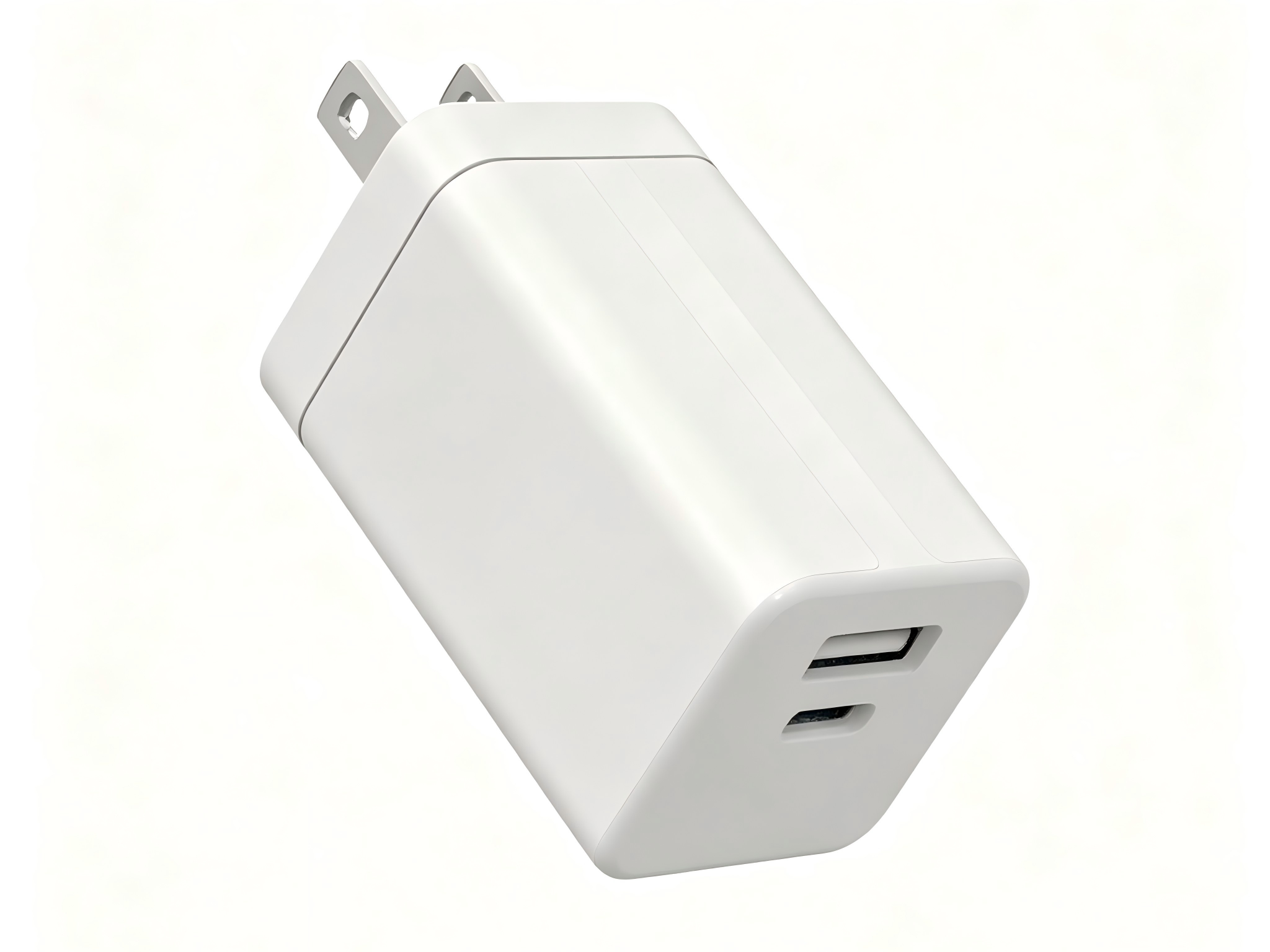
Enhancement-mode GaN devices in the GaN fast charger have thresholds within a few volts, clearly lower than silicon MOSFETs, so slight gate disturbance can enter the conduction region. In bridge or synchronous rectifier structures, dv/dt during fast turn-on of the complementary device couples through gate-drain capacitance into the gate of the GaN fast charger, and displacement current lifts gate voltage. Negative off-bias, larger turn-off resistance or active clamp driving improve immunity of the GaN fast charger.
2. Drive Voltage Window and Drive Loss
The upper drive limit of the GaN fast charger is narrow: exceeding the rating accelerates gate aging or causes breakdown, while too low a voltage raises on-resistance and heating. Drive loss of the GaN fast charger scales with gate charge, drive voltage and frequency, becoming significant at high frequency. The drive loop of the GaN fast charger needs regulation and clamping to prevent overshoot at start-up or load step.
3. Common-source Inductance and Kelvin Connection
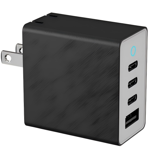
Package common-source inductance of the GaN fast charger generates back-EMF during switching, cancelling part of the drive voltage and slowing transitions. A Kelvin source connection separates drive and power loops in the GaN fast charger, reducing the effect of common-source inductance. Layout keeps the drive loop close, shortens gate traces and uses a dedicated drive ground so power current does not develop voltage across it.
4. Dead Time and Reverse Conduction Loss
The GaN fast charger has no conventional body diode; during dead time current flows in reverse through the channel with a higher drop than a silicon diode. Excessive dead time raises reverse conduction loss in the GaN fast charger, while too short a dead time risks shoot-through. Dead time of the GaN fast charger is set from device behaviour and drive propagation delay and rechecked over temperature, since delay drift at high temperature increases risk.
5. Drive Reliability Validation and Stress Screening
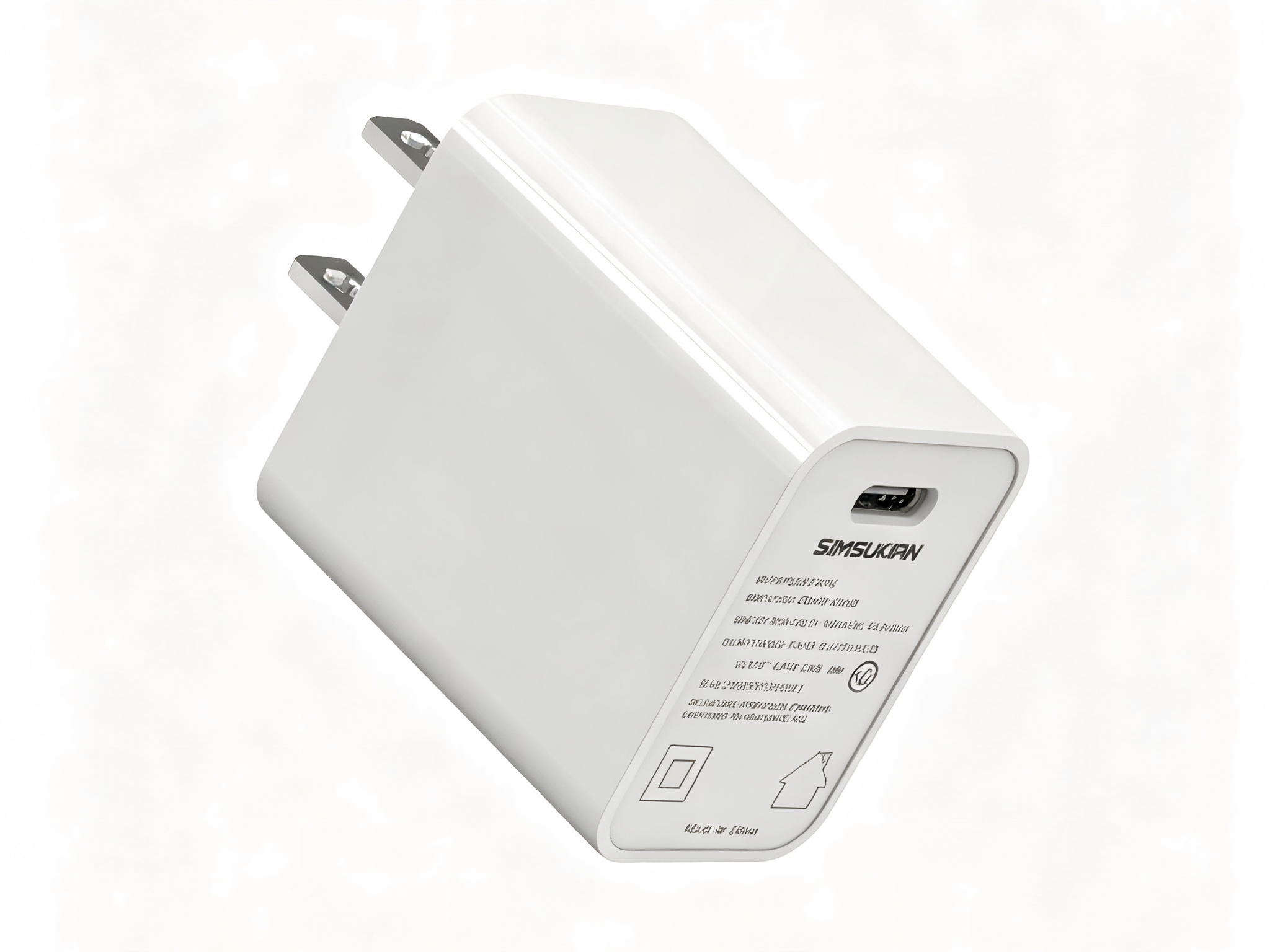
Drive reliability of the GaN fast charger is verified through repeated switching, extreme duty cycles and load steps, watching gate waveforms for ringing and overshoot. Device-level reliability of the GaN fast charger may follow JEDEC stress methods covering high-temperature reverse bias, high-temperature gate bias and thermal cycling. Production sampling of the GaN fast charger also checks gate waveforms and switching loss to contain efficiency and temperature variation from device batches.
Conclusion
Gate drive is an easily underestimated part of a GaN fast charger; false turn-on often appears only at temperature extremes and full load. Simsukian provides drive waveform debugging and stress assessment. Overseas buyers are welcome to contact Simsukian to confirm drive designs for the GaN fast charger.
FAQ
Q1: Are the certifications complete and verifiable?
A1: Simsukian’s full product range covers major certifications including UL, CE, FCC, PSE, KC, SAA, UKCA, and CB. All certificates can be verified through official channels, effectively avoiding risks of fake, borrowed, or expired certificates that may cause customs clearance failure or platform delisting.
Q2: How is the quality stability and protection performance?
A2: All Simsukian products undergo 100% aging tests and are equipped with multiple protections including over-voltage, over-current, short-circuit, and over-temperature protection. They feature low ripple, low heat generation, and an average lifespan of approximately 50,000 hours, supporting long-term full-load stable operation.
Q3: Can products be customized? What are the sample and mass production lead times?
A3: OEM/ODM customization is fully supported, including voltage, current, connector, plug type, housing, and logo. Sample lead time is 5 days. Standard bulk order lead time is 18–20 days. Sample fees are refundable after placing a bulk order.
Q4: Do the products meet energy efficiency and standby power requirements?
A4: The full range meets DOE Level VI and higher energy efficiency standards. Some models achieve no-load power consumption ≤0.1W, complying with ErP and other international energy-saving regulations.
Q5: How are lead time, MOQ, and after-sales service guaranteed?
A5: As a source manufacturer with abundant stock of standard models, delivery is stable. Standard warranty is 1 year (free repair within the first year). Lifetime repair support is provided; after the first year, appropriate material and labor fees will be charged.
References
1. Simsukian Official Website
2. JEDEC JESD47 Stress-test-driven qualification of integrated circuits
3. IEC 62368-1 Audio/video, information and communication technology equipment – Safety requirements
Power adapter
Power adapter
Related Articles More>>
- Energy Efficiency Test Standards and Loss Parameter Analysis for Desktop Power Adapter
- Peak Efficiency and Dynamic Load Parameters of silicon carbide power adapter for Data Center Servers
- Desktop Power Adapter: Technical Parameters, Specifications and Selection Guide
- Dynamic Load and Transient Response Technical Parameters of power adapter