

Abstract
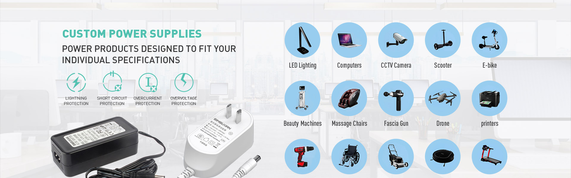
SiC devices in a SiC power adapter are rated to high junction temperature, but usable temperature of the SiC power adapter is limited by package, die attach and PCB. Junction calculation and heat path design decide whether the SiC power adapter delivers stable output.
1. Device Rating versus Package Limit
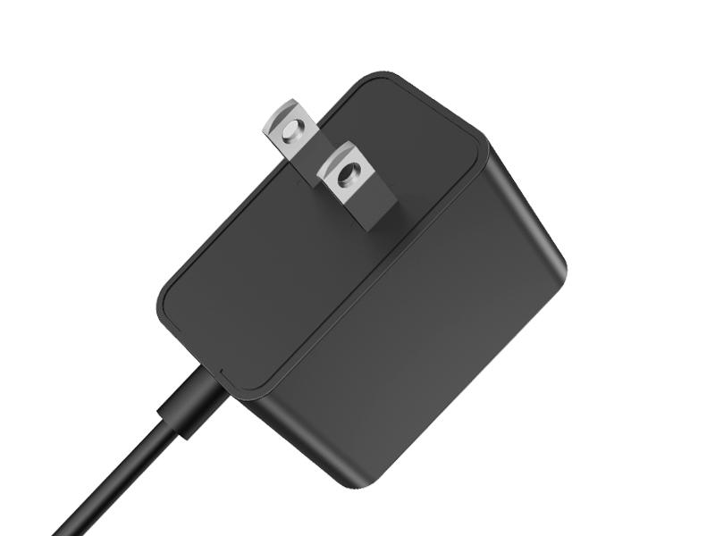
SiC MOSFETs in the SiC power adapter are typically rated near 175 degrees Celsius junction, well above common silicon. The real bottleneck in the SiC power adapter is often package material, die attach and molding rather than the die. Under sustained heat, voids in the die attach of the SiC power adapter grow and thermal resistance rises, creating a self-reinforcing temperature spiral.
2. Junction Calculation and Thermal Chain
Junction temperature of the SiC power adapter follows loss and the thermal chain: junction to case, case to pad, pad to PCB and PCB to ambient. Copper area, via count and layer count are key mid-chain resistances in the SiC power adapter, and device thermal data alone underestimates rise. The SiC power adapter should build a full model calibrated by measurement, especially in sealed housings where ambient resistance dominates.
3. Parameter Drift at High Temperature
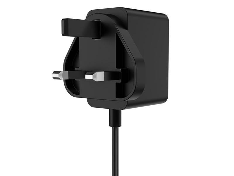
On-resistance of the SiC power adapter rises with temperature, increasing conduction loss and coupling with temperature rise. Threshold of the SiC power adapter falls as temperature rises, raising false turn-on risk and requiring margin in negative bias. Body diode drop also varies, so freewheeling loss must be calculated at high temperature.
4. Thermal Structure and Potting Process
The SiC power adapter transfers heat through thermal pads, gap fillers or potting to the housing, with conductivity and filler loading deciding effectiveness. Voids or incomplete fill in the SiC power adapter raise local resistance and create hot spots. Thermal design must respect safety spacing, since conductive materials crossing the insulation boundary would break coordination.
5. High-temperature Life and Thermal Cycling
Sustained heat ages die attach and molding of the SiC power adapter, requiring operating life tests at temperature. Thermal cycling may follow IEC 60068-2-14 to simulate expansion from on-off cycles and day-night swings in the SiC power adapter. After cycling, temperature rise, on-resistance and insulation of the SiC power adapter are re-measured to confirm no resistance increase or joint cracking.
Conclusion
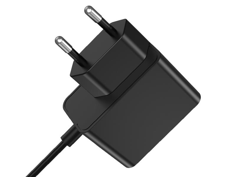
The high-temperature advantage of a SiC power adapter only materialises when package and cooling keep pace; junction management is the core constraint. Simsukian provides junction modelling and thermal cycling validation. Overseas buyers are welcome to contact Simsukian to confirm thermal designs for the SiC power adapter.
FAQ
Q1: Does Simsukian support OEM and ODM orders?
A1: Yes, Simsukian supports OEM & ODM customization, including logo, casing, parameter and packaging adjustment.
Q2: What certifications can Simsukian provide?
A2: Simsukian can provide CE, RCM, FCC, UL, CCC, KC/KCC, PSE, SAA certification certificates. The company holds ISO9001 and ISO14001 system certifications.
Q3: What is the sample lead time?
A3: Sample preparation takes 5 working days.
Q4: What trade terms can be accepted for cooperation?
A4: Simsukian supports FOB, and EXW can be discussed upon customer request.
Q5: What is the warranty period for the products?
A5: The product warranty period is 1 year.
References
1. Simsukian Official Website
2. JEDEC JESD51 Thermal measurement guidelines for semiconductor packages
3. IEC 60068-2-14 Environmental testing – Test N: Change of temperature
Power adapter
Power adapter
Related Articles More>>
- Temperature Rise & Aging Bench Test Analysis for Interchangeable Plug Power Adapter
- Technical Parameters of wall plug power adapter versus Desktop Selection
- USB Charger | ODM Custom 4-Port USB-A Commercial Hub, Per-port Current Limit & Hotel Power Solution
- Desktop Power Adapters: Technical Parameters and Specs US Buyers Must Verify